


SiGen Introduces High Volume Manufacturing Kerf Free Wafering Equipment
SAN JOSE, Calif.--(BUSINESS WIRE)--Silicon Genesis, a leader in process and technology for engineered substrates announced today that it has started production of solar wafers using its new high volume manufacturing PolyMax system. In an industry first, SiGen has produced 85μm thick, 156 mm square kerf-free monocrystalline silicon wafers. Kerf is the material converted into saw dust, inherent in all sawing processes. This achievement delivers the first true mono c-Si kerf-free wafering for the PV industry.
The introduction of the PolyMax high volume manufacturing system brings the industry one step closer to replacing wire saw processes with a lower cost waste-free wafering solution. A key strength of the PolyMax system is its ability to produce wafers thinner than is achievable with wire saw technology, allowing the industry to produce cells with higher conversion efficiencies and lower cost.
“We believe the benefit of using kerf-free wafers will allow the PV industry to reach unsubsidized grid parity. The start up of our high volume manufacturing system is a key step towards achieving this goal,” said Francois Henley, CEO of SiGen.
In an invited talk at the 35th IEEE PV Specialists Conference, Henley reviewed crystalline silicon kerf-free wafering technologies. At the upcoming 25th European Photovoltaic Solar Energy Conference and Exhibition (25th EU PVSEC) in Valencia, Spain, SiGen will present the PolyMax production system (2CV.1.53).
About SiGen
Silicon Genesis Corporation (SiGen) is a leading provider of engineered substrate process technology for the semiconductor, display, optoelectronics, and solar markets. SiGen’s technology is used for production of Silicon-On-Insulator (SOI) semiconductor wafers for high performance applications. SiGen develops innovative substrates through thin-film engineering, enabling new applications and markets for its customers. SiGen's customers and partners include top players from substrate and device suppliers throughout the world. Founded in 1997, SiGen is headquartered in San Jose, California. For more information on Silicon Genesis, visit http://www.sigen.com
Photos/Multimedia Gallery Available: http://www.businesswire.com/cgi-bin/mmg.cgi?eid=6415938&lang=en
Contacts
Silicon Genesis
Alessandro Fujisaka, 408-228-5858
afujisaka@sigen.com
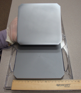
PolyMaxTM - 85um thick wafer - 156mm x 156mm.(Photo: Business Wire)